Add to Cart
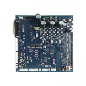
High Tg Custom Pc Boards FR4 Printed Circuit Board Manufacturer
FASTPCBA is highly skilled at helping customers transition from consignment and turnkey system manufacturing that includes all components procurement and consulting service.
With over 20 years experience years in EMS field, we build-up a strong relationship with our supplier chain who have commited on our works and will to make our business successful together.
1. 100% Brand New Parts from Reliable Source
2. 100% IQC inspection
3. Suppliers Chain Management & MRP System
4. Rapid lead time
5. Passive and Active components are available
6. RoHS and SGS compliance

| Technology Capabilities | |
|---|---|
| Layer | 1~48L |
| Min.inner Layer Trace | 0.076mm |
| Min.inner layer Space | 0.076mm |
| Min.outer Layer Trace | 0.076mm |
| Min.outer Layer Trace | 0.076mm |
| Max.inner layer copper Thickness | 6oz |
| Max.outer layer copper Thickness | 14oz |
| Layer to Layer registration tolerance <10L | +/-0.076mm |
| Layer to Layer registration tolerance >10L | +/-0.125mm |
| Max.Finished board thickness | 8mm |
| Min.Finished board thickness | 0.3mm |
| Min.Core Dielectric thickness | 0.051mm |
| Min.Impedance-Differential | +/-5% |
| HDI Stack up | 1+N+1,2+N+2,3+N+3 |
| Controlled Depth Drilling Tolerance | +/-0.1mm |
| Advanced | Buried cpacitor,buried Resistor,Embedded coin,rigid -flex,Rigid- Flex+HDI,Rigid-flex+Metal Base |
| Max Production Panel Size | 24.5"*43" |
| Via in PAD | YES |
| BGA Pitch(with trace) | 0.4mm |
| Soldermask Registration | +/-0.03mm |
| Min.Solder Dam | 0.064mm |
| Min.Drilled Hole size-Mechanical | 0.2mm |
| Min.Drilled Hole size-Laser | 0.1mm |
| Max.Laser Drill Aspect Ratio | 20:01 |
| Press Fit Hole | +/-0.05mm |
| Layer To layer Registration Tolerance | 0.04mm |
| Min.Dielectric Thickness | 0.04mm |
| Controlled Depth Drilling | YES |
| BGA Pitch(with trace) | 0.5mm |
| surface Finishing | ENIG,OSP,Immersion tin,immersion silver,HASL,Electrolytic gold, |
| Materil | Normal TG,Middle Tg,High Tg,Halogen free,Low Dk Laminate, High Frequency Laminate,PI Laminate,BT Laminate |

Millions of circuit boards are produced here every year, which provides superior service for automotive electronics, medical electronics, power communications, industrial automation, intelligent home and other industries around the world. We will continue to improve our quality and service; customer satisfaction and development of science and technology are our eternal motivation.

FAQ:
Q: What files do you use in PCBA fabrication?
A: Gerber or Eagle, BOM listing, PNP and Components Position
Q:Is it possible you could offer sample?
A: Yes, we can custom you sample to test before mass production
Q: When will I get the quotation after sent Gerber, BOM and test procedure?
A: Within 6 hours for PCB quotation and around 24 hours for PCBA quotation.
Q: How can I know the process of my PCBA production?
A: 7-10 days for PCB production and components purchasing, and 10 days for PCB assembly and Testing
Q: How can I make sure the quality of my PCBAs?
A: We ensure that each piece of PCBA products work well before shipping. We'll test all of them according to your test procedure. Also if there are any defect items during the shipping, we also can be free to repair for you.